VR SOP Training for PCB Fabrication

Relevant case studies

Blog post: 05/11/2025 11:38 am
 Author: Spark Team
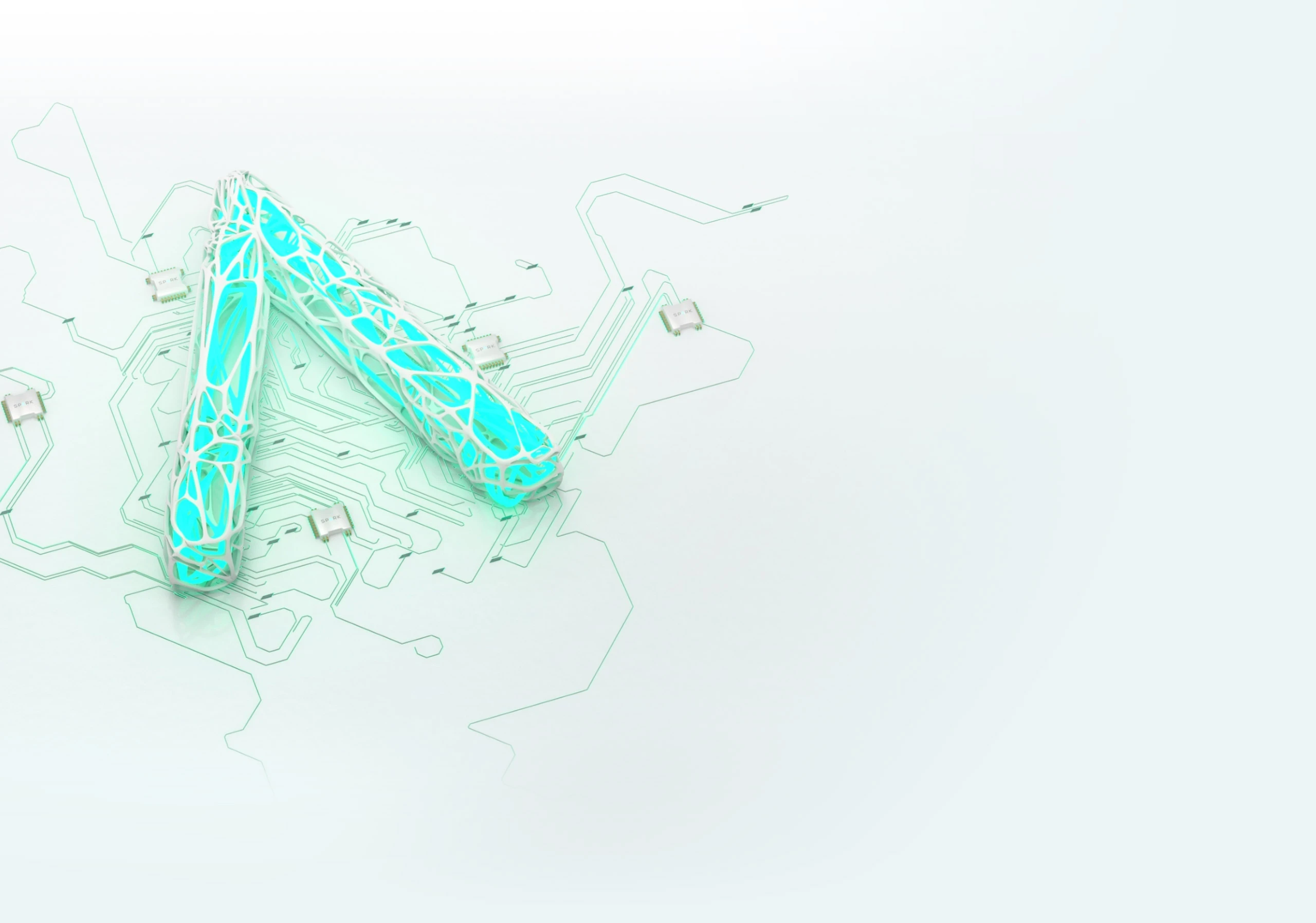
VR SOP Training for PCB Fabrication
Make imaging, plating and drill/route routines easy to learn and repeat
PCB fabs rely on disciplined chemistry and accurate tooling. Spark designs bespoke VR training that mirrors your inner/outer layer imaging, etch/strip, PTH/ENIG/OSP lines, lamination, drill/route and AOI—so operators practise the right sequence safely.
Typical challenges
- Imaging/registration: artwork alignment, UV dose and resist thickness.
- Chemistry control: etch rate, copper thickness, pH/ORP and bath life.
- Lamination: stack-up accuracy, pressure/temperature and void control.
- Mechanical: drill hit accuracy, burr control, routing and cleanliness.
Our bespoke build approach
- Capture SOPs & limits: process windows, SPC charts and inspection criteria.
- Create scenarios: panel prep, imaging, plating, lamination and drill/route set-ups.
- Coach in VR: prompts aligned to your travellers and QA gates.
- Assess: right-first-time, defect hotspots and rework drivers.
Benefits
- Fewer scrap panels and re-makes.
- Stable thickness/registration across shifts.
- Cleaner audits with clear training evidence.
Why Spark
We encode your stack-ups, chemistries and standards—training that maps to your fab.
See a PCB VR SOP demo. Contact Spark.
© 2026 All Rights Reserved | Company Reg No. 05327622 | Spark Emerging Technologies Limited